VLSI Lab 5 - VGA Controller (Compiled & working on Quartus v20.1)
VLSI Lab 5 - VGA Controller
(To be compiled on Quartus v20.1)

Figure 1 VGA Controller Block Diagram (Click to enlarge)
Running PolyU remote-desktop access UDS: https://puuds.polyu.edu.hk/uds/page/login
Please check the availability of the lab: https://www.eie.polyu.edu.hk/it/lab/cf502/
Datasheet file of Video DAC: https://www.analog.com/media/en/technical-documentation/data-sheets/adv7123.pdf
You could understand the principle from the above website of eewiki.


(extracted diagram
from the user manual of DE1-SoC)
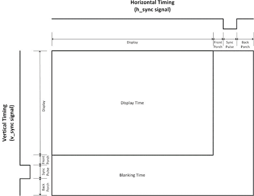
VGA Signal Timing Diagram
Pin assignment of the I/Os to connect to control the video DAC chip:

Files:
1) Design Verilog file VGA1_V.v : https://drive.google.com/file/d/1XA12FW6gY6i8q_aLBuW4yIvcuavr6OSD/view?usp=sharing
2) Pin assignment file VGA1_V.qsf : https://drive.google.com/file/d/1xmFU5P9cUuAP6X_dg25MHAfdfF8WSGYL/view?usp=sharing
3) Test bench file tb_VGA1_V.v : https://drive.google.com/file/d/1C-1IxXAUH36I-q7cOLEceGjnl1iYo1WM/view?usp=sharing
4) 7zipped project folder file (640x480): https://drive.google.com/file/d/1lntxDAnVw766DBw3JzQZKdAHOMsLrPf7/view?usp=sharing
Hardware test with development board DE1-SoC

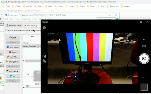
(Click to enlarge picture)
Simulation using Modelsim
Compile the verilog files and the test bench file.

C:\intelFPGA_lite\20.1\quartus\eda\sim_lib\altera_mf.v
(my installation folder is "c:\intelFPGA_lite\20.1" and you need to change if it is different)
Then locate the compiled test bench (tb_VGA1_V) under the work library (double-click it):
(my installation folder is "c:\intelFPGA_lite\20.1" and you need to change if it is different)
Then locate the compiled test bench (tb_VGA1_V) under the work library (double-click it):

You can find the signals in design unit i1:

(click to enlarge)
Select the signals and add them to the waveforms:

The wave transcript is as:
vsim work.tb_VGA1_Vadd wave -position insertpoint \sim:/tb_VGA1_V/i1/CLK \sim:/tb_VGA1_V/i1/RST_N \sim:/tb_VGA1_V/i1/VCLK \sim:/tb_VGA1_V/i1/VGA_SYNC \sim:/tb_VGA1_V/i1/VSYNC \sim:/tb_VGA1_V/i1/HSYNC \sim:/tb_VGA1_V/i1/BLANK \sim:/tb_VGA1_V/i1/VGA_R \sim:/tb_VGA1_V/i1/VGA_G \sim:/tb_VGA1_V/i1/VGA_B \sim:/tb_VGA1_V/i1/clk_div2 \sim:/tb_VGA1_V/i1/hPos \sim:/tb_VGA1_V/i1/vPos \sim:/tb_VGA1_V/i1/hs \sim:/tb_VGA1_V/i1/vs \sim:/tb_VGA1_V/i1/de \sim:/tb_VGA1_V/i1/pll_clkout \sim:/tb_VGA1_V/i1/pll_locked \sim:/tb_VGA1_V/i1/SYNCrun 5000000

(Click to enlarge)

Then the waveform window shows:

(Click to enlarge)
The horizontal position counter (hPos) increases at the rising edge of the pixel clock (VCLK) and the vertical position counter (vPos) increases when the horizontal position counter overflows:

(Click to enlarge)
The VGA RGB output changes at about 35 us:

(Click to enlarge picture)

(Click to enlarge)
The verilog design file can be modified by:
1) Changing parameters according to the synchronization signals required by the VGA standard:
2) Adding a digital phase-lock loop (DPLL / PLL) under the top module to generate a required pixel clock (e.g. 65 MHz in 1024x768@60Hz)
Below is the modified verilog file:
// ----- The Hong Kong Polytechnic University //// ----- EIE511 Project Sample - VGA Controller //
module VGA1_V (CLK, RSTN, VGA_CLK, VGA_VS, VGA_HS, VGA_BLANK_N, VGA_SYNC_N, VGA_R, VGA_G, VGA_B);
input CLK; // System Clock Input (FPGA)
input RSTN; // System Reset Signal (FPGA active low)
output VGA_CLK; // VGA Pixel Clock
output VGA_SYNC_N; // VGA Sync Signal
output reg VGA_VS; // VGA Vertical Sync (vsync) Signal
output reg VGA_HS; // VGA Horizontal Sync (hsync) Signal
output reg VGA_BLANK_N; // VGA Blank Input
output [7:0] VGA_R; // VGA 8-bit Red Input
output [7:0] VGA_G; // VGA 8-bit Green Input
output [7:0] VGA_B; // VGA 8-bit Blue Input
parameter HD = 16'd1024; // Horizontal Resolution (640)
parameter HFP = 16'd24; // Right border (front porch)
parameter HSP = 16'd136; // Sync Pulse (Re-trace)
parameter HBP = 16'd160; // Left boarder (back porch)
parameter HPOS_MAX = HD + HFP + HSP + HBP - 1; // Calculation of H-Position Max.
parameter VD = 16'd768; // Vertical Display (480)
parameter VFP = 16'd3; // Right border (front porch)
parameter VSP = 16'd6; // Sync pulse (Retrace)
parameter VBP = 16'd29; // Left boarder (back porch)
parameter VPOS_MAX = VD + VFP + VSP + VBP - 1; // Calculation of V-Position Max.
// reg clk_div2 = 0; // Internal Register for Divide-by-2 Clock
wire pixel_clk;
reg [15:0] hPos = 0; // Register for current Horizontal Position Storage
reg [15:0] vPos = 0; // Register for current Vertical Position Storage
reg hs = 0; // register for hsync generation (account for pixel data delay)
reg vs = 0; // register for vsync generation (account for pixel data delay)
reg de = 0; // register to indicate current position is in drawing area or not
// outputs
assign VGA_SYNC_N = 0;
assign VGA_CLK = pixel_clk; //clk_div2;
//assign pixel_clk = clk_div2;
/* // PLL Instantiation */
PLL PLL_inst
(
.refclk(CLK) , // input refclk_sig
.rst(~RSTN) , // input rst_sig
.outclk_0(pixel_clk) // output outclk_0_sig
// .locked(pll_locked) // output locked_sig
);
// Clock Divided by 2
//always @(posedge CLK) clk_div2 = ~clk_div2;
// Horizontal_position_counter (clk_div2, RSTN)
always @(posedge pixel_clk, negedge RSTN) begin
if (RSTN == 0)
hPos <= 0;
else if (pixel_clk == 1)
//hPos <= (hPos == (HD + HFP + HSP + HBP - 1)) ? 0 : (hPos + 1);
if (hPos == HPOS_MAX)
hPos <= 0;
else
hPos <= hPos + 1;
end
// Vertical_position_counter:process(pixel_clk, RSTN)
always @(posedge pixel_clk, negedge RSTN) begin
if(RSTN == 0)
vPos <= 0;
else if (pixel_clk == 1)
if (hPos == HPOS_MAX)
if (vPos == VPOS_MAX)
vPos <= 0;
else
vPos <= vPos + 1;
end
//Horizontal_Synchronisation:process(pixel_clk, RSTN)
always @(posedge pixel_clk, negedge RSTN) begin
if(RSTN == 0) begin
hs <= 1;
VGA_HS <= 1;
end
else if (pixel_clk == 1) begin
if((hPos >= (HD + HFP)) && (hPos < (HD + HFP + HSP)))
hs <= 0;
else
hs <= 1;
end
VGA_HS <= hs; //delay one clock to account for pixel data delay
end
//Vertical_Synchronisation:process(pixel_clk, RSTN)
always @(posedge pixel_clk, negedge RSTN) begin
if(RSTN == 0) begin
vs <= 1;
VGA_VS <= 1;
end
else if (pixel_clk == 1) begin
if((vPos >= (VD + VFP)) && (vPos < (VD + VFP + VSP)))
vs <= 0;
else
vs <= 1;
end
VGA_VS <= vs; //delay one clock to account for pixel data delay
end
//video_on:process(pixel_clk, RSTN)
always @(posedge pixel_clk, negedge RSTN) begin
if(RSTN == 0) begin
de <= 0;
VGA_BLANK_N <= 0;
end
else if (pixel_clk == 1) begin
if ((hPos < HD) && (vPos < VD))
de <= 1;
else
de <= 0;
end
VGA_BLANK_N <= de; //delay one clock to align with pixel data
end
//module for drawing horizontal colorbar:process(pixel_clk, RSTN)
draw_colorbar_v #(.HD(HD), .VD(VD)) inst_draw (
.CLK(pixel_clk),
.RSTN(RSTN),
.R(VGA_R),
.G(VGA_G),
.B(VGA_B),
.de(de),
.hPos(hPos),
.vPos(vPos)
);
endmodule
----- ----- ----- ----- -----
Below is another version of creating two sqaures in the resolution of 1024x768:
1) VGA2_V.v verilog file: https://drive.google.com/file/d/1kCLcYZ4wxpyQDjDL4SM23okwcGD79oNI/view?usp=sharing
2) sq.v verilog draw file: https://drive.google.com/file/d/1CsT_ZBLrjTchBg6EA-kXWeYBbyx61yXt/view?usp=sharing
3) sync.v verilog file: https://drive.google.com/file/d/1CsT_ZBLrjTchBg6EA-kXWeYBbyx61yXt/view?usp=sharing
4) vga2_v.qsf pin assignment file: https://drive.google.com/file/d/1aWaMWaacTWfUdFCr6UqYX7ubsscIEbb6/view?usp=sharing


5) Outcomes on the VGA monitor:
(Click to enlarge the photo)
(Click to enlarge the photo)


留言
張貼留言