VLSI Lab 1: Design of Combinational Logic Designs using Schematic entry and Verilog using Quartus Prime
VLSI Lab 1
Lab 1: Design of Combinational Logic Designs using Schematic entry and Verilog using Quartus Prime
Laboratory Objectives
The objectives of this laboratory are:
- Learn how to use a commercially available FPGA synthesis environment.
- Create a combination circuit using graphical design entry (schematic entry) and Verilog.
- Analyze the synthesis results and understand the FPGA resources consumed.
- Simulate the design generating a testbench and verify the correctness of the simulation.
Introduction
This is a step-by-step tutorial for building a 1-bit full-adder using Quartus II Design Suite software that provides designers with the ability to generate digital circuits in different ways, e.g. schematic entry and/or using a hardware description language such as VHDL or Verilog. The Quartus II also provides the ability to apply FPGA pin and timing constraints, analyze for errors and violations.
Full Adder
An example 1-bit full adder block diagram and Boolean circuit are shown below with its truth table (to be completed at your report).
Select the FPGA board DE1-SoC. It is easier to configure the project.Full adder schematics:
Change Project Navigator to "Files" and Right click on Files to add fulladder.v to your project.
Setting the Verilog file as top entity and recompile the design.
The console window illustrates where the testbench has been generated.
Rename the file to a verilog type file (e.g.) "fulladder_tb.v" and add it to your project in Quartus.
Open and edit test-bench fulladder_tb.v as shown below to define input test vector A, B and Cin. The file is attached here for you to download.
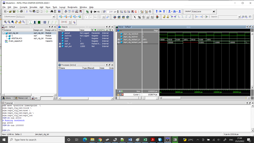
Run a simulation: Tools > Run Simulation Tool > RTL Simulation
Problem 1:
Solve 1:
Tools > Options > (Find under) General > EDA Tool Option
Specify the simulation tools path where e.g. C:\intelFPGA_lite\20.1\modelsim_ase\win32aloem (in our lab PC)
Assignments > Settings > (Find under) EDA Tools Settings > Simulation > ModelSim-Altera > Verilog (See below)
Then, run a simulation: Tools > Run Simulation Tool > RTL Simulation
After doing so, Modelsim simulator could be started with above settings. To compile testbench : Compile -> Compile…
Choose the file "fulladder_tb.v" .
Click compile and then click done. This will create an entry in the work library.
Right click on fulladder_tb and choose simulate. Then select the signals to be displayed and drag to
Waveform.
Increase simulation step from 100ps to 1000ps and start simulation.
(Right click the signal and choose "Add Wave". You can type a command: e.g. run 1000000)


留言
張貼留言